Exploring a Smart Thermostat
I was doing some tidying up and stumbled upon this “smart” thermostat that never got installed, and decided to take a poke at it.
Basically, you connect it to your home’s heating/cooling system where it provides a user interface via its touch display. You can additionally connect it to your home wifi network for remote access capabilities through the Resideo Total Connect Comfort app.
As for why it’s Resideo and not Honeywell, it seems like Resideo spun off from Honeywell back in 2018 and handles all of the connected home climate control and security aspects for Honeywell.
Initial Reconnaissance
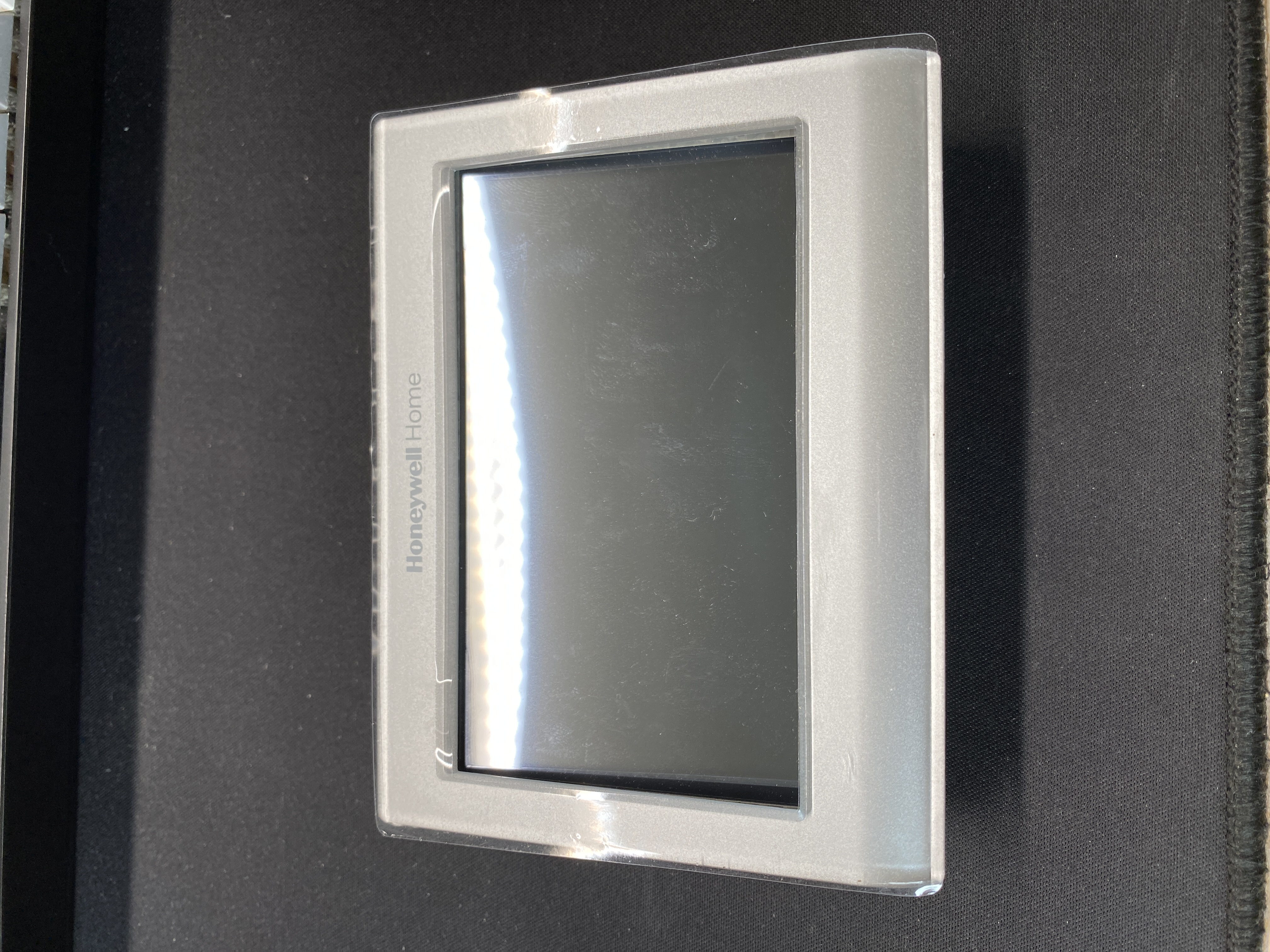
Front
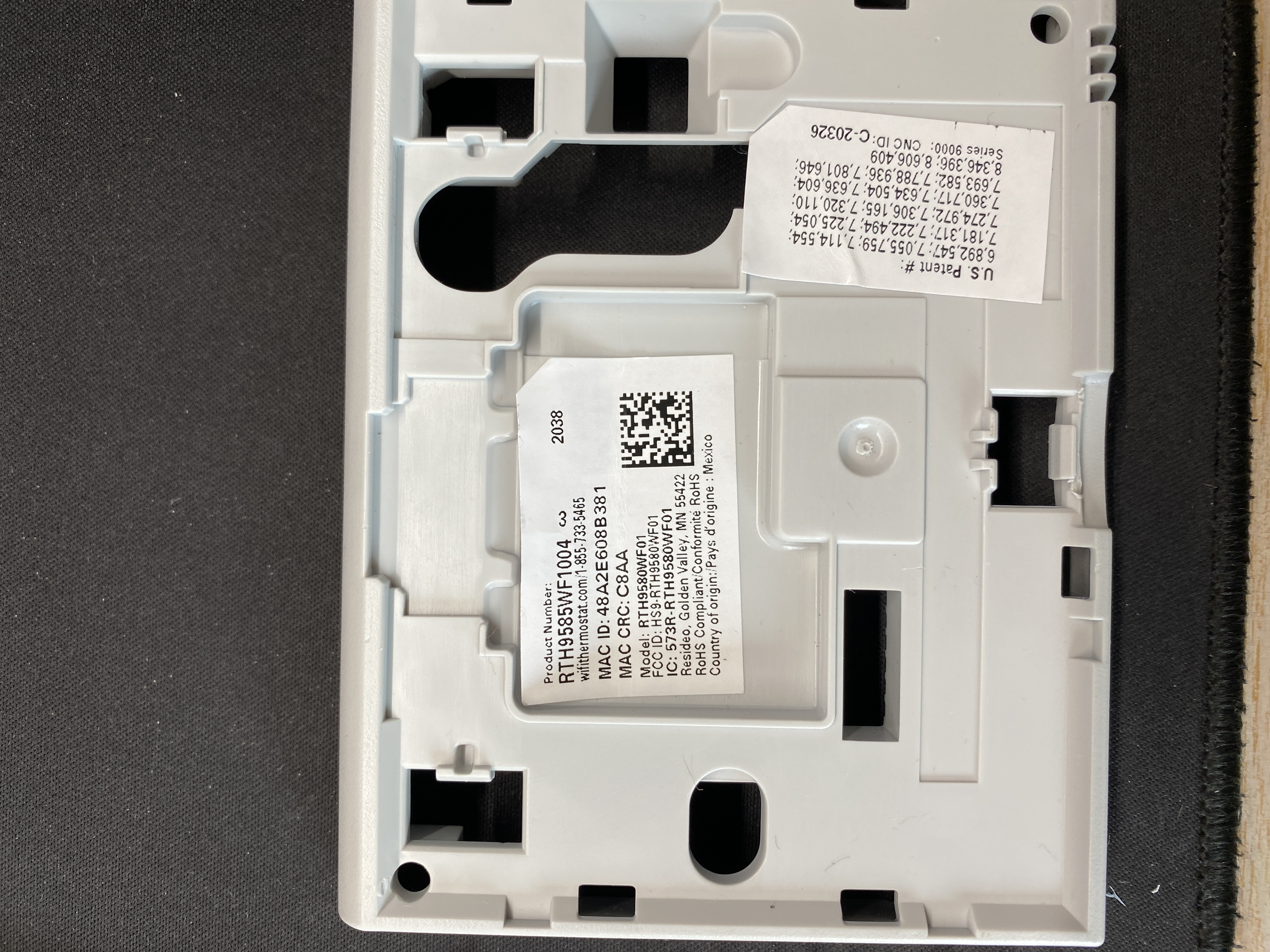
Back
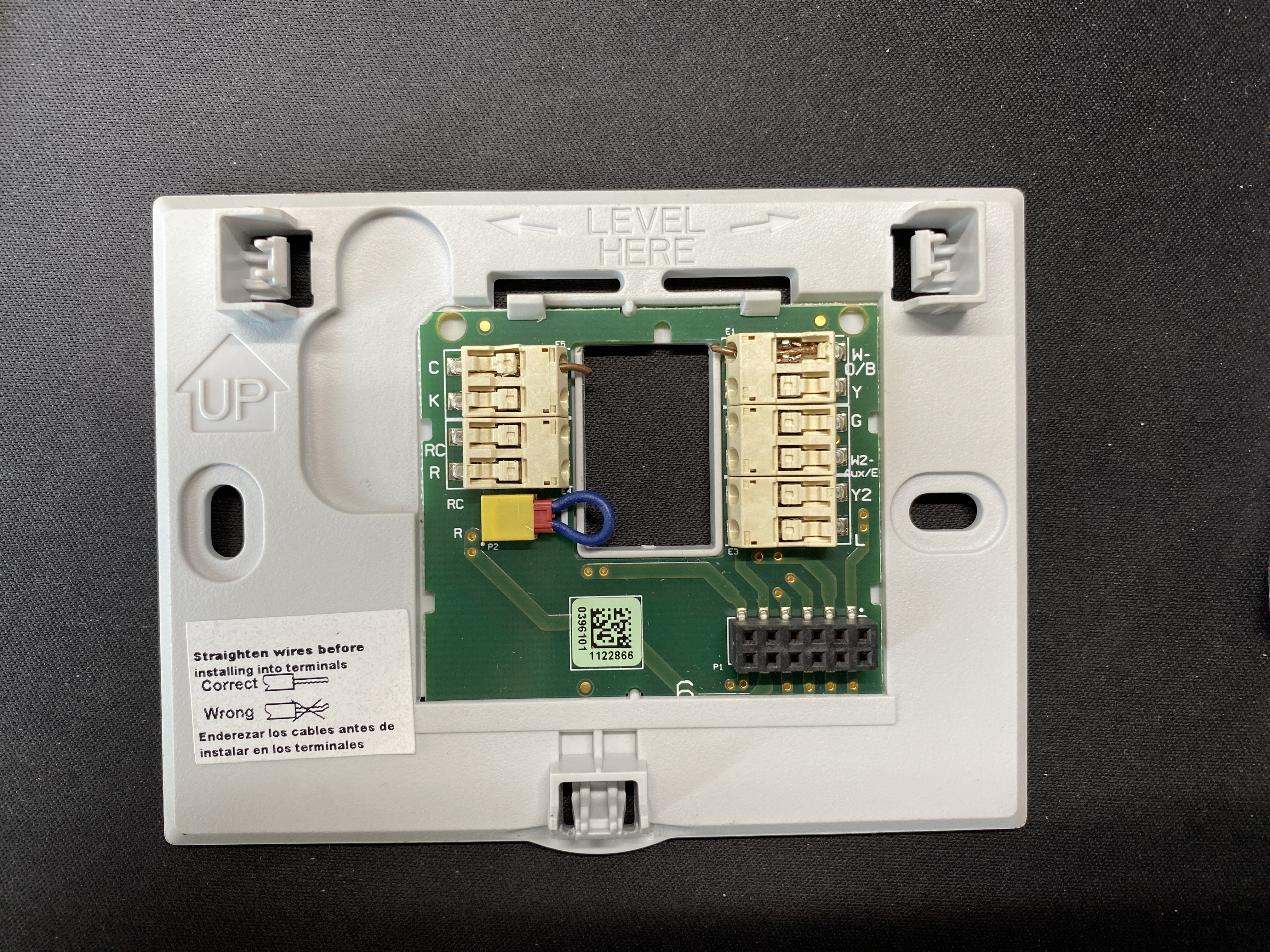
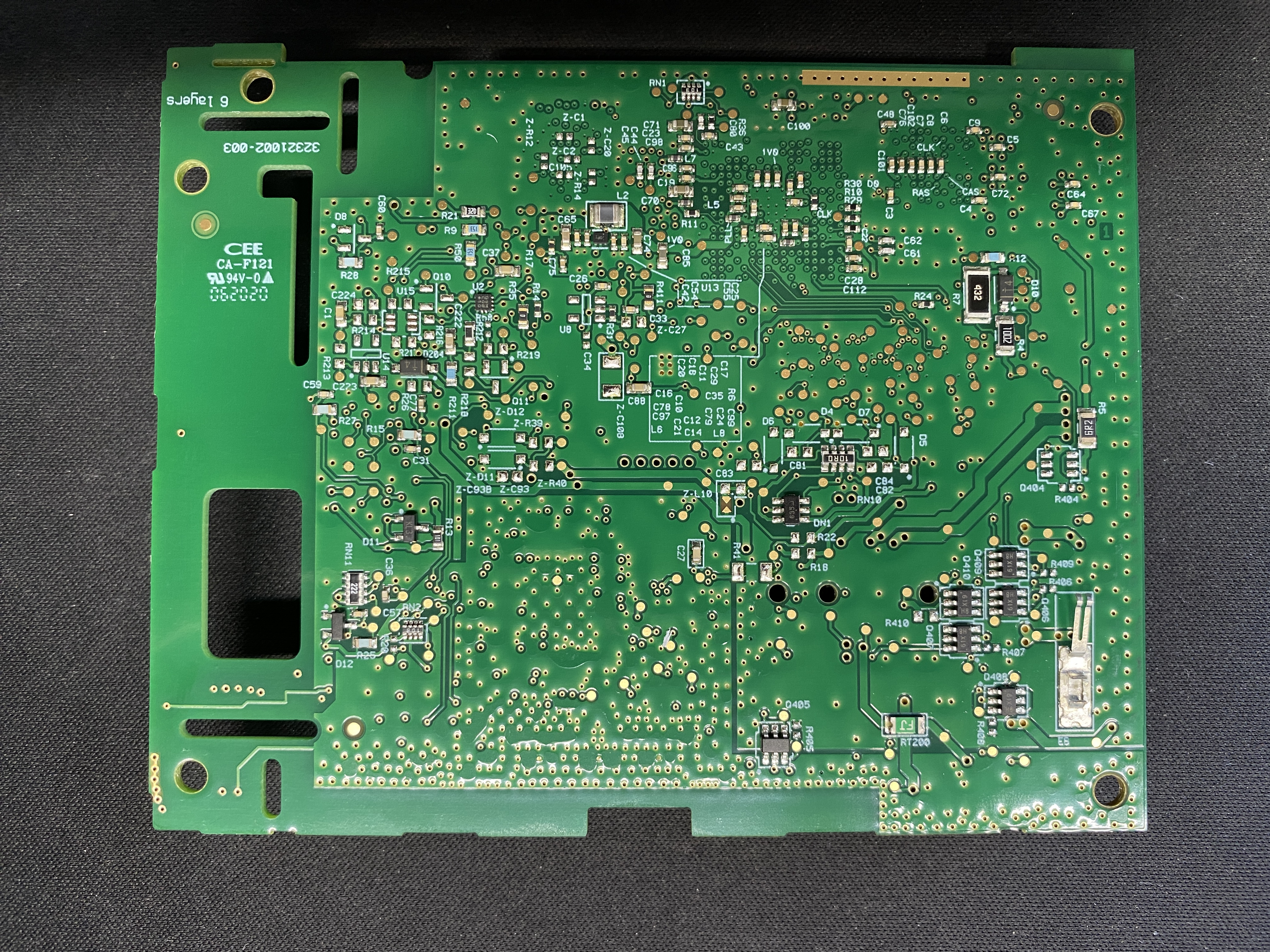
Connector plate
Of course, nothing’s fun without cracking it open and seeing the guts in all their entirety. Opening it up was relatively easy with just clips that you could undo with a spudger. The touch screen display is held to the main PCB via a ribbon cable.
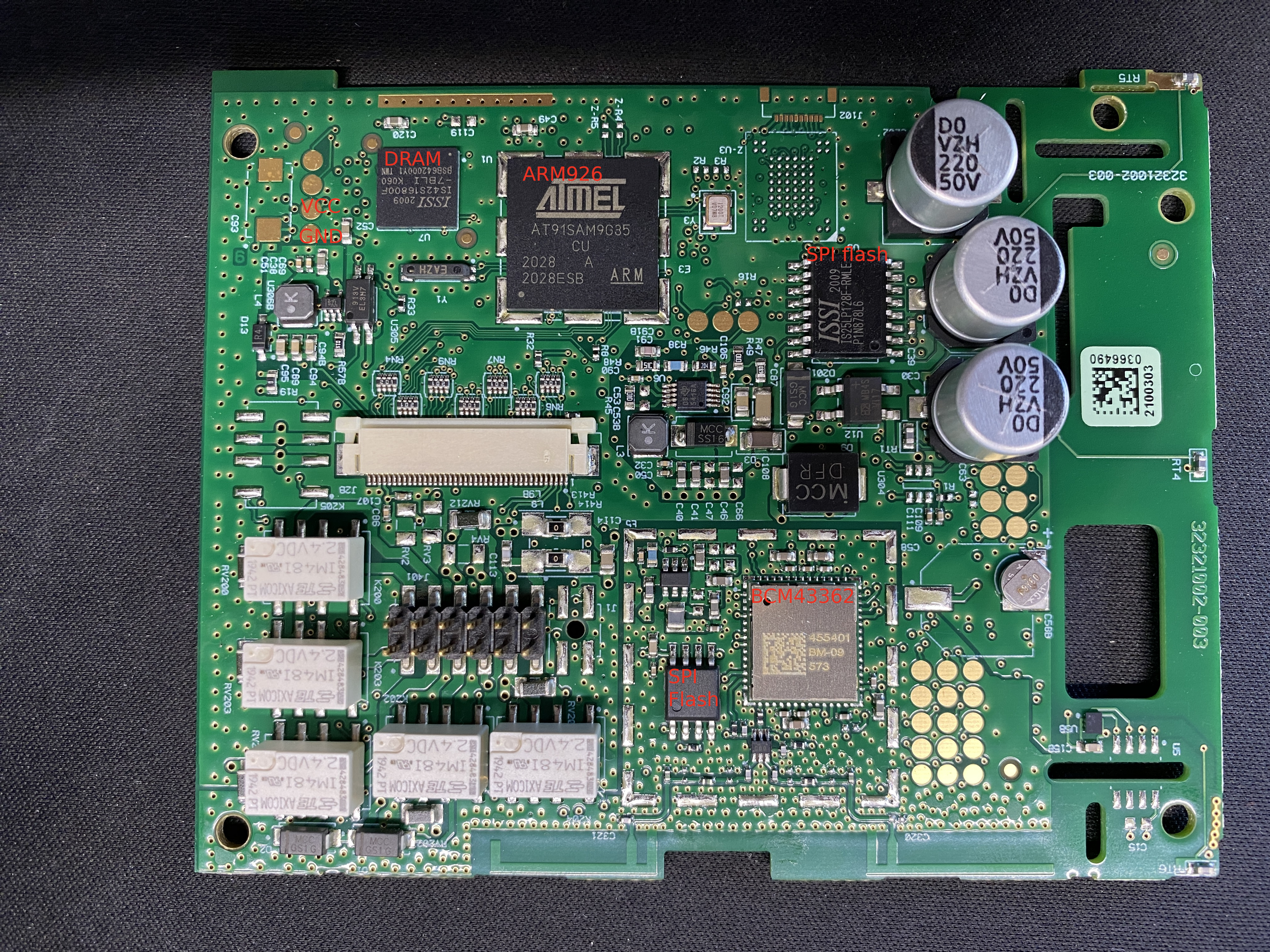
We can speculate on the purpose of some of these components. The giant Atmel MPU is the main processor that has an LCD controller for touch screens and network connectivity capabilities like ethernet and CAN, according to the datasheet. The DRAM is physically close to the MPU for quick access during device operation.
The wifi module may be a Broadcom BCM43362, which would be capable of 2.4GHz(1) 802.11 b/g/n single band wifi. Searching for the chip label didn’t provide many results, though the main result is for a WM-N-BM-09, which is what I went with. If this nomenclature can be trusted, FCCID(2) also has additional info on what could be an alternative form factor of this module, with pictures of what’s under the shield.
Finally, there are two SPI flash chips on here; a SOIC16 and the more common SOIC8 chip for storing non volatile information. These are the most interesting to me because they almost certainly hold firmware, which we can extract and explore for clues of the underlying functionality. The larger SOIC16 flash with its proximity to the MPU is probably for storing the bootloader, main OS, and any relevant assets for operation. The smaller SOIC8 flash chip is right next to the wifi module, perhaps with its own firmware and software, or for storing configuration info such as SSIDs and PSKs for connectivity(3).
One thing I was curious about was what the footprint for the J102 label on the silkscreen could be for. Initially I was thinking it could be some weird form of USB for debugging, but someone pointed me to an older internal teardown photo on FCCID, which showed a type of ribbon connector. It looks like it may connect to some kind of BGA IC for interfacing for debugging/programming purposes during development, and unfortunately does not seem to be immediately useful to us right now.
There are also a lot of test points on the device, which could indicate interfaces like JTAG, SWD, or UART. Sweeping some of these points with a multimeter in continuity mode showed the presence of VCC and GND pins next to label C25 in the top left. The two other pads next to it look like they could be the TX/RX points for a UART connection(4).
Summary
- Model: Honeywell RTH9585WF1004
- FCCID: https://fccid.io/HS9-RTH9580WF01
- Atmel AT91SAM9035 ARM926 MPU
- Broadcom BCM43362 + STM Cortex-M3 (maybe)
- ISSI IS25LQ032B 32Mb SPI flash memory
- ISSI IS25LP128F-RMLE 128Mb SPI flash memory
- ISSI IS42S16800F DRAM
- TE Axicom IM481 relay 2.4VDCB
Powering the Device
So obviously the next thing I wanted to do was to power the device on and see how it works. After a bit of digging into how to wire up thermostats, it became clear that I needed 24V AC voltage to run the device, which I don’t have just lying around on my desk.
To give a bit of background, non-smart thermostats don’t normally have power continuously running through them, and only connect the heater signal when required. Smart thermostats however always need power to work, requiring what’s called the common wire, also known as the C-wire, which provides a return through the R-wire for continuous power. This voltage gets transformed into DC power and downconverted into a voltage an embedded system can handle, which is typically from 1.8V to 5V.
Some smart thermostats like the ubiquitous Nest thermostats use a technique called “phantom power” or “power stealing” to trickle charge a battery or a super capacitor by rapidly turning on and off the HVAC system. It’s a cool idea, but can cause problems for some HVAC systems.
This is all to say that there was no defined input voltage and ground point immediately visible to me where I wanted to start randomly applying voltages. I could try to find where the voltages get transformed into DC voltages by reverse engineering the power section of the board, starting probably next to the input pin headers and the relays, or next to the capacitors, but I don’t feel confident yet in my abilities to do that correctly.
So, shelving the idea of trying to turn it on until I have a cheap 24V AC power supply on hand. However, I know that once I do have a power supply I just need to connect it to the C-wire terminal and the R-wire terminal on the thermostat, and that should be enough to power the device.
Dumping SPI Flash
The next thing we can do with the device itself is dump the SPI flash chips I was looking at earlier. In order to speak SPI to a target chip, I could use a programmer like the FTDI 2232H. I have a Tigard I’ll be using, which is an awesome multiprotocol tool based on the FT2232H.
SPI Overview
Sparkfun always has great explanations, but to summarize, SPI is a synchronous communication protocol. Unlike asynchronous protocols like UART, it requires having a clock signal to drive communication, where received or sent bits are read on the rising or falling edges of the clock. In addition, a chip select line wakes the device up right before being used.
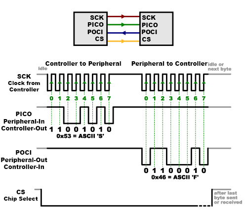
Based on this, we have at least four signal lines we have to connect, besides ground and maybe VCC:
- CLK - Needed to synchronize and drive the communication.
- COPI(5) - Controller out peripheral in.
- CIPO - Controller in peripheral out.
- CS/CE - Chip select or chip enable.
- GND - Pretty much any time you’re wiring something up you should have this connected if it’s available.
- VCC - ONLY if the device is OFF! If the device is powered already, leave this disconnected. Tigard also has a handy ability to set the target supply voltage, so that’s something you have to look up on a case by case basis. Both SPI chips in this case are 3.3V, so we can leave it on that, so long as the device is off when we’re talking directly to the chips.
Typically, the term controller in these situations means the main microcontroller being used to talk to the peripheral. This should guide your wiring as well, where you connect the microcontroller’s TX line to the peripheral’s RX for COPI, and vice versa.
SOIC16 Flash
With that said, we can start wiring up our programmer to the SPI flash. The first target is the SOIC16 flash which is an 128 Mb ISSI IS25LP128F. Scanning through the datasheet shows us the pinouts for each package type they have. Since we have the SOIC16 one, that’s what we’ll reference in our wiring.
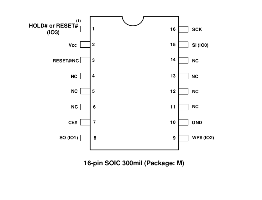
Wiring goes like this then:
| Programmer | Flash IC |
|---|---|
| VCC (at 3.3V from data sheet) | VCC (pin #2), with the device off |
| CS/CE | CE# (pin #7) |
| CIPO | SO (pin #8) |
| GND | GND (pin #10) |
| COPI | SI (pin #15) |
| CLK | SCK (pin #16) |
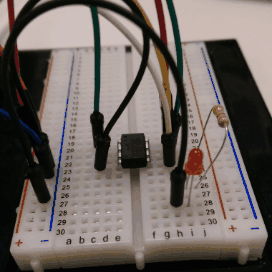
My wiring looked something like this after all was said and done:
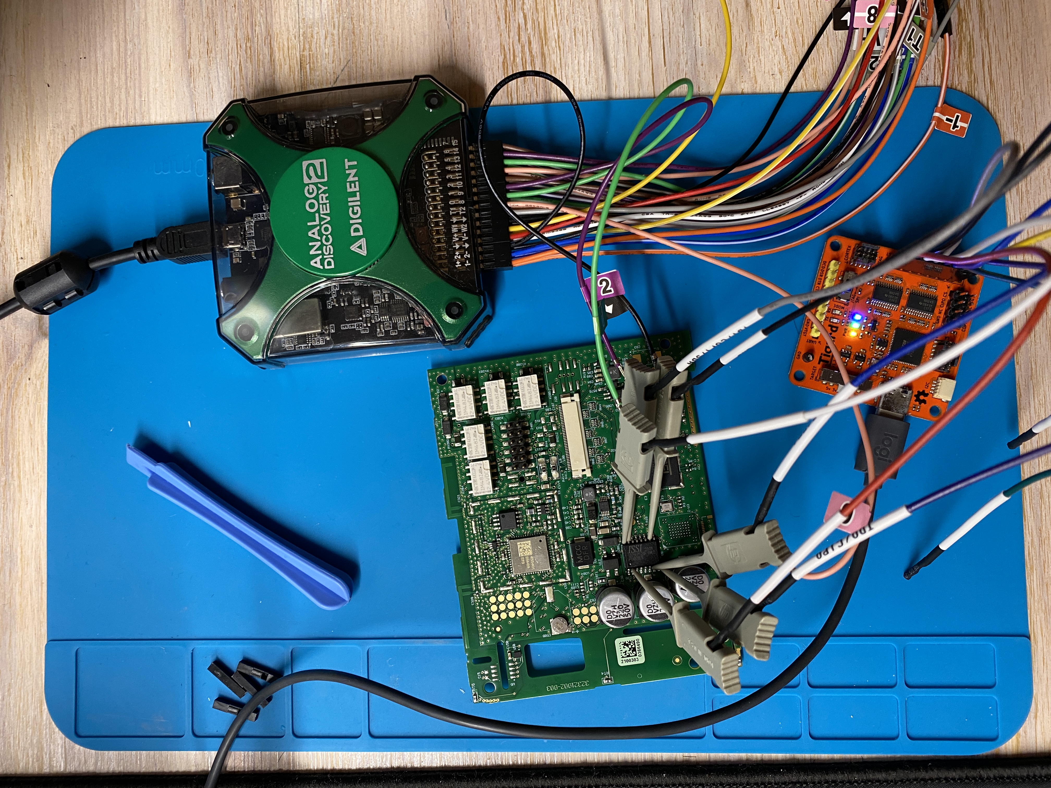
I also connected my Analog Discovery 2 to sniff the lines as I was reading the device. Mostly, I wanted to get more usage out of my AD2 for fun as it doesn’t get enough action. :)
Chatting to Flash #1
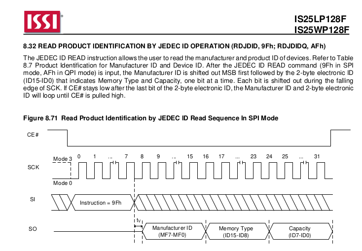
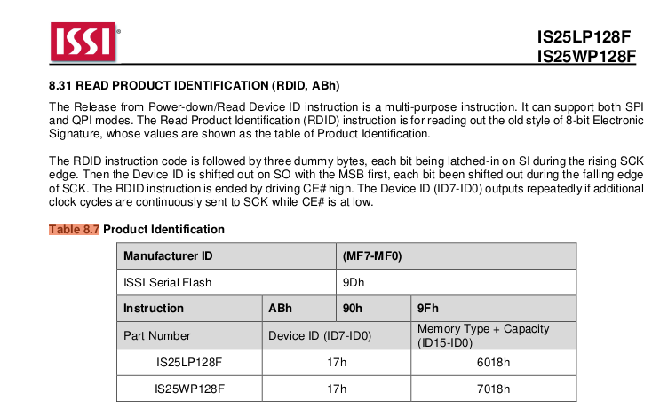
We can send and receive data directly now that everything’s set up to go. One of the ways we can get started is issue a sort of “hello world” by asking the device for its device ID, or JEDEC ID. Typically this is done by issuing the command 0x9F to the peripheral. In the product sheet, we can see that in SPI mode we can send 0x9F and receive three bytes back, with each byte being the manufacturer ID, memory type, and capacity in that order.
We can write a Python script to send this command using the PyFtdi library. We can modify the Tigard example to give us the following script below:
from pyftdi.ftdi import Ftdi
Ftdi.show_devices()

from os import environ

ftdi_url = environ.get('FTDI_DEVICE', 'ftdi://ftdi:2232:TG11006b/2')

from pyftdi.spi import SpiController, SpiPort
ctrl = SpiController()
ctrl.configure(ftdi_url)
ctrl.flush()
spi = ctrl.get_port(cs=0, freq=1E6, mode=0)

jedec_id = spi.exchange([0x9F], 3)
print(jedec_id)
This is Tigard specific, but our script is choosing to use the second port on the Tigard for interfacing.
We then configure our SPI interface to use a frequency of 1MHz, and mode 0(6) according to the data sheet.
Finally, spi.exchange sends a Python list of bytes, and returns a specified number of bytes returned from the peripheral.
In our case it’s three bytes, since that’s what the data sheet says we’ll get in response to our 0x9F command.
Running this with our Tigard connected should give us something like this output:
$ python read_id.py
Available interfaces:
  ftdi://ftdi:2232:TG11006b/1       (Tigard V1.1)
  ftdi://ftdi:2232:TG11006b/2       (Tigard V1.1)
  ftdi://ftdi:232h:210321AD5987/1   (Digilent USB Device)

bytearray(b'\x9D\x60\x18')
Comparing our result to Table 8.7 from the datasheet matches an IS25LP128F chip, which is what we have.
This is helpful for giving a sort of first pass on checking if a device works (dark foreboding ahead here).
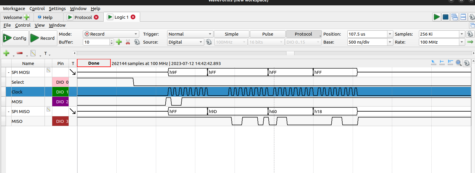
Using our AD2 with Digilent’s Waveforms logic analyzer function shows us a nice readout to confirm our device functionality.
Dumping Flash Chip #1
So that’s cool and all, but how about dumping the entire SPI flash? We could continue with scripting with Python and PyFTDI (and I may write about this later), but there’s a program that we can use to cheese this called flashrom. Flashrom is an open source project that basically compiles support for many kinds of flash chips for common operations such as writing, reading, or erasing.
We can try running flashrom directly to see if it detects the flash chip like this (tailored for Tigard’s FTDI 2232H since that’s what I’m using):
$ flashrom -p ft2232_spi:type=2232H,port=B,divisor=4
Luckily for us, flashrom correctly identifies this particular IS25LP128F, meaning we should be able to start using it out of the box.
$ flashrom -p ft2232_spi:type=2232H,port=B,divisor=4
flashrom v1.2 on Linux 5.19.0-32-generic (x86_64)
flashrom is free software, get the source code at https://flashrom.org

Using clock_gettime for delay loops (clk_id: 1, resolution: 1ns).
Found ISSI flash chip "IS25LP128" (16384 kB, SPI) on ft2232_spi.
No operations were specified.
We can also check the source code to see if it’s supported, supposing we’re using the latest version that’s on there. Here we can find it on their Github in include/flashchips.h.
If we want to read the flash to a file in order to dump it, we use the -r flag followed by the name we want to give the binary, i.e.
$ flashrom -p ft2232_spi:type=2232H,port=B,divisor=4 -r is25lp128-dump.bin
It’s a good idea to dump the flash a few times and compare the hashes to confirm its integrity.
With the dump on hand, we can run strings to get a first pass on what we’re facing.
$ strings -n10 is25lp128-dump.bin | less
----- Manhattan UI2 Thermostat Bootloader %.2x.%.2x.%.2x.%.2x -----
+ Compiled: %s %s
Aug  3 2017
+ MCK:      %d MHz
Checking AC power level...
%05d,%d...
-I- Status or ID mismatch
|*******|-- 005
|*******|-- %s
Public Key
|*******|-- 003
|*******|-- 004
-I- I cache enabled.
-I- I cache is already enabled.
-E- Device not detected or unknown
AT25DF041A
AT26DF081A
AT26DF0161
AT26DF161A
AT25DF512B
SST25VF512
02003MANH01-0000
echo Manhattan wifi uart test message test of 430 Rx,Tx communication
...
Seems like there’s a lot of interesting stuff to explore!
Binwalk gives us a few guesses as to what’s going on in here as well.
$ binwalk is25lp128-dump.bin

DECIMAL       HEXADECIMAL     DESCRIPTION
--------------------------------------------------------------------------------
18480         0x4830          SHA256 hash constants, little endian
2466367       0x25A23F        LZMA compressed data, properties: 0x5A, dictionary size: 100663296 bytes, uncompressed size: 144 bytes
3070740       0x2EDB14        TIFF image data, little-endian offset of first image directory: 3801088
3335107       0x32E3C3        eCos RTOS string reference: "ecos:"
4498746       0x44A53A        eCos RTOS string reference: "ecos del sistema"
4502988       0x44B5CC        XML document, version: "1.0"
Note that binwalk can and will give you lots of false positives, as it’s just checking for any matches to known file signatures. A quick way to check is see if the last digit is odd, which could indicate the result is not aligned in a typical way. So these results are not very reassuring, and I can say that the LZMA result also did not actually produce anything meaningful.
We can also check to see if there’s any kind of encryption or compression going on here with:
$ binwalk -E is25lp128-dump.bin
This gives us an entropy graph of the binary.
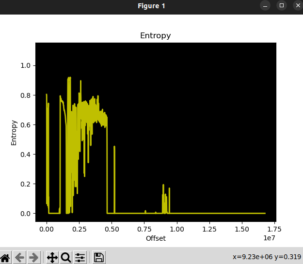
This doesn’t look to me to be encrypted or compressed and seems to be just data. Something that’s encrypted/compressed in contrast will stay at the very top of the entropy graph rather than have these sporadic oscillations. Next steps probably involve throwing it into a disassembler like Ghidra to see if we can make sense of it, though I’ll have to reserve that for another post.
Additionally, I have also tried dumping that SOIC8 flash chip mentioned earlier, which resulted in a whole set of complications that I’ll have to also set aside writing about for now.
So stay tuned for potentially more followup posts about this project!
-
Almost all IOT devices only use 2.4GHz wifi modules, probably for cost saving measures along with 2.4GHz band’s inherent ability to travel further for low data applications. Browsing Amazon reviews for IOT devices will almost always bring up a handful of 1-star reviews complaining of the inability to connect their smart home device to their network, which I believe could be due to newer routers defaulting to using only 5GHz band connectivity. ↩
-
FCCID is an amazingly useful resource for initial recon, as they have teardown photos and frequency info from FCC compliance testing. Since almost all connected devices in the US have to pass FCC regulations, you’ll likely find a good majority of devices on there. Even if you don’t have the device on hand, it’s very useful for getting a peek under the hood as sometimes you can get an idea of what kind of debug headers they sometimes left on the test device, or if they left chip labels on before removing them in production. ↩
-
The presence of the footprint of a shield surrounding the flash and the wifi module also adds to the theory that the flash’s intended purpose is to support the wifi module. Small details like that help give a more cohesive idea of what developers may have had in mind when designing the system. ↩
-
If you’re looking for UART pins, you can look for test pads or unpopulated headers in sets of four as an easy first pass. Doing a multimeter sweep in continuity mode helps narrow down VCC and GND to known sources, leaving just figuring out which one could be TX and RX. When you boot the device, you can try seeing if you get any data from either of the two points while tweaking the baud rate. If you get legible text, you’ve found the device’s TX and can designate the other as RX. If you have any exposed pins to a known nearby microcontroller that could be providing UART to the suspected pins, you can try tracing them in continuity mode to confirm their functionality as well. ↩
-
Previously these were known as MOSI/MISO standing in for “master” and “slave”. Recently this has changed for the more acceptable “controller” and “peripheral” terminology, and is IMO clearer as well. However you will doubtless see the MOSI/MISO terminology in older datasheets, so something to be aware of. ↩
-
Mode is basically when to sample data on the clock signal, with mode 0 being the rising edge of the clock. The data sheet will tell you which one to use specifically for your operation. ↩